.svg)

Every technology field has a moment when proprietary infrastructure gives way to open standards, and the players who recognize the transition early define what comes next. In quantum computing, that moment has arrived for the control stack.
National labs and programs are committing capital at a scale the field has not seen before. Universities are building quantum engineering programs that need infrastructure. Industry is pushing past proof-of-concept and asking what a utility-scale quantum system actually requires in practice. The hardware has matured. Qubit coherence times have improved by orders of magnitude. Fabrication processes are being standardized.
What the ecosystem needs now is a common, open control platform, one that any lab can adopt, any program can standardize on, and any vendor can build on top of. Not a proprietary stack that locks you in. Not a research prototype that lives on one group's GitHub. A platform with the community mass and technical credibility to become the de facto standard for quantum control.
The Quantum Instrumentation Control Kit (QICK), developed by Fermilab and now commercialized in partnership with Qblox, is the most serious candidate for that role available today.
Whether you are a researcher pushing the limits of gate fidelity or an industry leader scaling to utility-scale systems, here is why QICK is becoming the de facto standard for quantum control.
What is QICK?
The Quantum Instrumentation Control Kit (QICK) is an RF control and readout system developed by engineers at Fermi National Accelerator Laboratory under the US Department of Energy's Quantum Information Science program, in collaboration with university research groups and industry partners, and every layer of it (firmware, software, and hardware) is fully open source.
Since QICK was first published in 2022 (Stefanazzi et al., Rev. Sci. Instrum. 93, 044709), it has been adopted across the field — over 77 academic papers now report results obtained with QICK (link to QICK readthedocs papers page https://docs.qick.dev/latest/papers.html). The QICK platform directly synthesizes carrier frequencies above 10 GHz using higher Nyquist zones, without analog mixers, simplifying the hardware stack considerably.
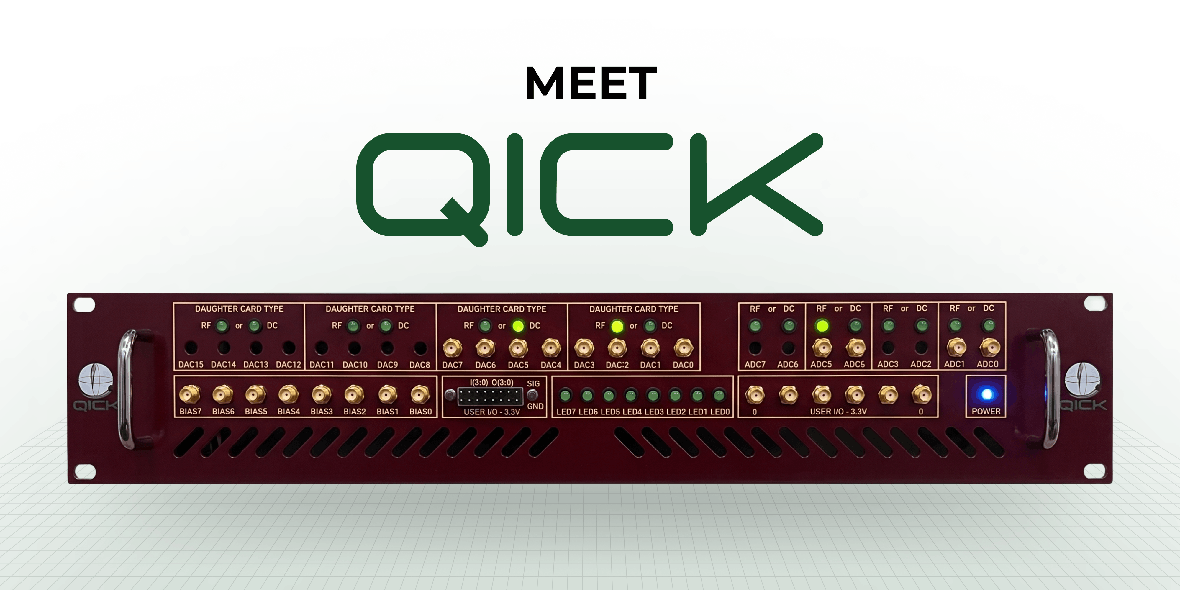
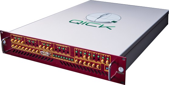
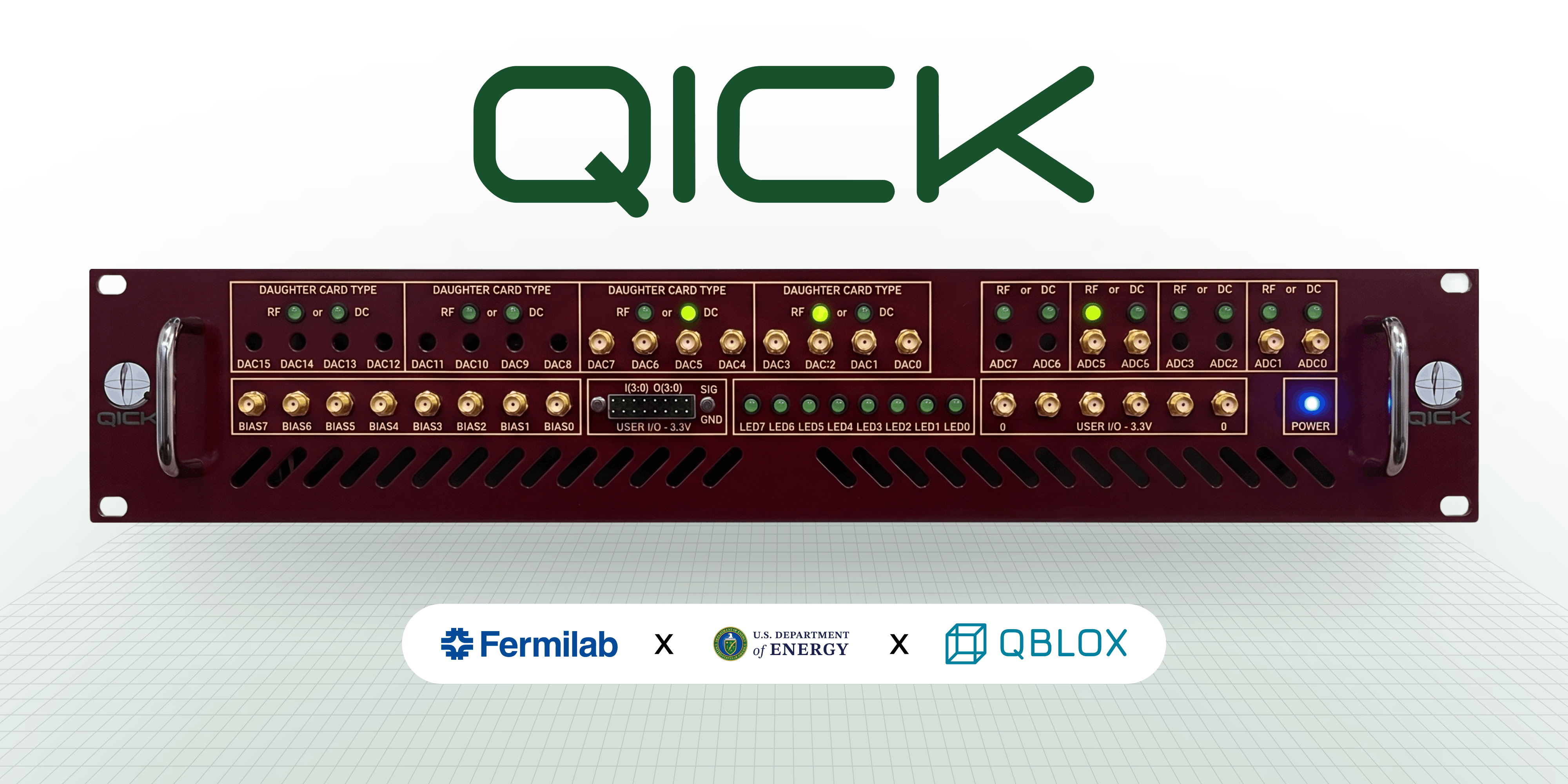
Today, with over 350 registered users across superconducting, spin, trapped-ion, and cold-atom (AMO) qubit platforms, QICK has become the most widely deployed open-source quantum control platform. The QICK box, a compact, fully integrated readout and control system with 32 RF/DC channels, is now production-ready.
QICK architecture: FPGA-based quantum control without analog upconversion
QICK is built on AMD's RFSoC (Radio Frequency System-on-Chip) platform, integrating CPU, FPGA, and RF data converters on a single chip. The key distinction from traditional quantum control setups: everything happens on the FPGA, with no CPU latency in the control loop.
The data converters operate at high enough sampling rates to synthesize microwave pulses directly. Using the second and third Nyquist zones, QICK DAC outputs extend past 10 GHz without any analog upconversion — which means no IQ mixers, no local oscillators, no sideband calibration, and no LO leakage. For the majority of superconducting qubit and readout cavity frequencies, the entire upconversion stage that dominates conventional control stacks simply does not exist in QICK. Instead, QICK uses direct digital synthesis to bypass analog upconversion.
On the FPGA side, pulse sequences, parameter sweeps, and feedback protocols execute entirely within the programmable logic, under the control of a custom-timed processor core. There is no round-trip to the host CPU between shots, no operating system scheduler introducing jitter, and no communication latency in the feedback path. The FPGA handles the experiment. The ARM processor and the Python interface handle configuration and data retrieval.
Sub-microsecond feedback for real-time error correction
Eliminating the CPU from the real-time control loop reduces feedback latency to the sub-microsecond range — the regime relevant to quantum error correction with superconducting qubits.
How easy is QICK to work with?
QICK’s user interface is written in Python and runs on AMD's open-source RFSoC-PYNQ framework, which provides direct programmatic access to firmware blocks and RFSoC hardware registers. Experiments are written as Python classes in a Jupyter notebook environment, either on a PC communicating with the board over the network, or directly on the board's built-in Jupyter server. There is no proprietary IDE, no compiled binary you cannot inspect, and no hardware abstraction layer that hides what the FPGA is doing.
This is a meaningful distinction for researchers who want to understand and control every aspect of their experiment. You can write a standard pulse sequence in a few lines of Python. You can also, if needed, modify the firmware and reload it between experiments with a single Python command. The depth is there when you need it; it does not get in the way when you don't.
Built on a strong foundation
The hardware substrate is AMD's RFSoC product line — a commercially supported, actively developed family of chips that AMD has committed to for the long term. The current primary board for QICK is the ZCU216, which hosts the ZU49DR RFSoC with 16 DAC channels at up to 9.85 GS/s and 16 ADC channels at up to 2.5 GS/s. This is not a custom chip or a research prototype; it is a standard commercial evaluation board available through AMD's distribution network.
The software environment is AMD's RFSoC-PYNQ framework, which provides a ready-built Linux OS image with full hardware support for the data converters, memory interfaces, and peripheral buses. Setting up a functional QICK system does not require writing device drivers or bringing up a Linux kernel from scratch. The toolchain is maintained by AMD. The QICK-specific firmware and software stack sits on top of it as a separable layer.
The combination matters: a community-developed open-source control system, running on commercially supported hardware, maintained by a team at a major US national laboratory, with a growing network of institutional users who have a stake in its continuity. That is a more durable foundation than most research software achieves.
How flexible is QICK?
QICK's firmware is modular by design. Rather than a fixed configuration, the FPGA fabric is populated with firmware blocks (signal generators, readout channels, digital I/O, bias controllers) that can be selected, configured, and combined depending on what a given experiment requires. All blocks are compatible with all supported boards, and the software layer automatically detects the firmware configuration at runtime. Changing the firmware for a different experiment does not require rewriting the user-level Python code.
At the core of every QICK configuration is the timed-processor, a custom processor core that runs experiment programs. The timed-processor is not constrained to simple pulse sequences. It supports loops, conditional branches, register arithmetic, and parameter sweeps, all executing in the FPGA with deterministic timing. An experiment that needs to sweep a frequency, branch on a measurement result, and adjust pulse parameters in response can express all of that in a single program that runs entirely on the hardware, without Python involvement between shots.
Beyond the core stack, QICK is explicitly designed as a kit, a base layer that different communities can extend for their specific needs. Extensions exist for spin qubit platforms, NV-center defect control, neutral atom experiments, and integration with higher-level quantum programming frameworks. The architecture was designed from the start to support this kind of growth without requiring changes to the core firmware.
Getting started with QICK: documentation, office hours, and direct engineer access
Documentation that covers only the happy path is not actually useful for experimental physics. QICK's documentation is written to get a new user from board setup to running standard qubit measurements. The intent is that a researcher who has never used an RFSoC board before can reach first qubit data without needing to contact anyone for help.
For the cases where you do need to contact someone, QICK maintains a public support channel and runs weekly office hours with the core development team. QICK also offers direct access to the engineers who wrote the firmware. For a field where debugging a control system problem can stall an entire experimental campaign, that kind of support infrastructure is not a minor benefit.
Building the next generation of users
QICK runs on AMD's University Program RFSoC4x2 kit, a lower-cost board in the same RFSoC family, well-suited to small-scale experiments, course demonstrations, and teaching environments where having sixteen DAC channels is less important than having a system that is affordable, well-documented, and directly compatible with the full QICK stack.
In 2024, the QICK team used this platform to develop and teach a hands-on course on qubit readout at the US Quantum Information Science Summer School at Oak Ridge National Laboratory, with AMD University Program support. The full course materials, including lecture slides, lab notebooks, and firmware configurations, are publicly available on GitHub. A researcher or instructor who wants to build a qubit control curriculum on QICK does not need to start from scratch.
The graduate students and postdocs learning quantum control on QICK today are the PIs, lab directors, and industry engineers of the next decade. Building familiarity with a common platform at the educational stage has historically been one of the most durable ways a technology achieves ecosystem dominance.
How do you deploy QICK in your lab?
The gap between "the FPGA firmware works" and "I can connect this to my dilution refrigerator and run a qubit experiment" involves a significant amount of RF signal conditioning hardware that most evaluation boards do not include. The QICK box closes that gap.
The concept is deliberately minimal in its assembly steps:
- Purchase the ZCU216 evaluation board from AMD through standard distribution channels.
- Load the QICK firmware and software onto the RFSoC — a process covered step-by-step in the QICK documentation.
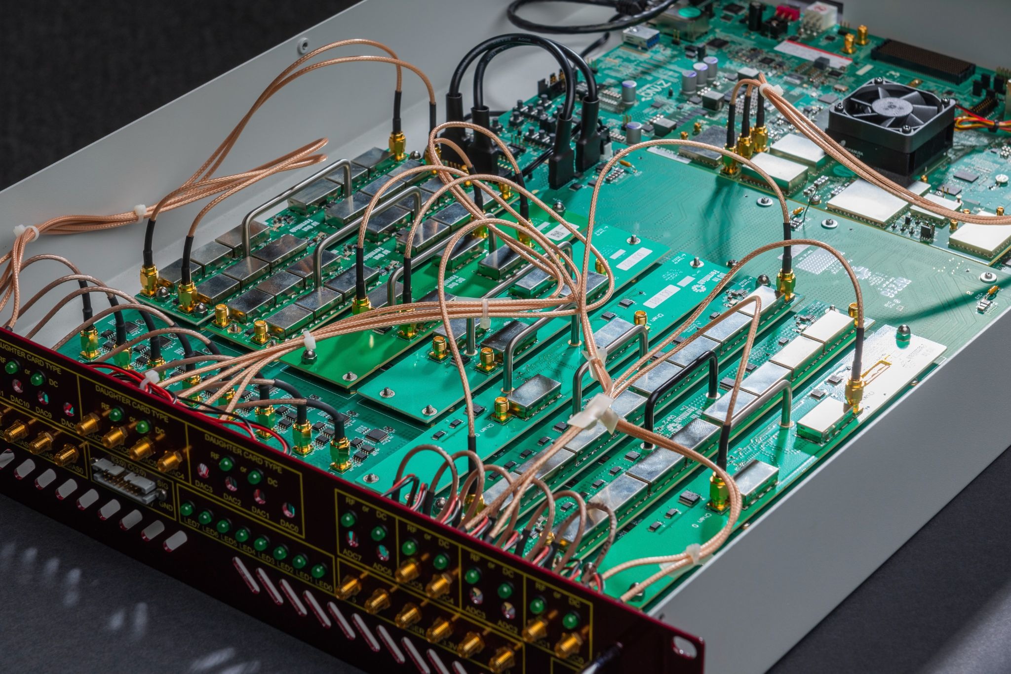
- Mount the Fermilab-designed RF216 main board and daughtercards — a custom modular RF, DC, bias, and I/O frontend with programmable filtering and attenuation, designed to mate directly with the ZCU216.
- Connect to the cryostat and run.
The modular daughtercard architecture is what makes the QICK box genuinely platform-agnostic. RF in and out cards, DC-coupled input and output cards, bias cards, and balun cards can be configured to match the signal conditioning requirements of different qubit types without modifying the main board or the firmware. Swapping a set of daughtercards for a different experiment is a hardware reconfiguration, not a system rebuild.
Full specifications
The QICK box provides a complete signal chain from room temperature to cryostat interface. The specifications below reflect the fully populated system.
- DAC Outputs: 16 channels. RF complex modulation up to 10 GHz, or unmodulated baseband from 0–1.5 GHz. No analog mixers required — mode is user-selectable per channel.
- RF Inputs: 8 channels, frequency range 0.5–10 GHz. Digital down-conversion on all channels, no analog mixers in the readout path.
- Bias Outputs: 8 channels, ±10 V, based on 20-bit DACs. White noise floor: 7 nV/√Hz , sufficient for flux-tunable and gate-defined qubit platforms.
- Digital I/O: 6 TTL I/O on SMA connectors. 8 TTL I/O on a separate connector. 8 LEDs for functional status display.
- Power: Under 70 W fully populated, from a single 12 V supply. Rack-mountable form factor.
The absence of analog mixers in both the output and input paths is the specification that matters most for calibration overhead. Digital down-conversion on the readout side means the same calibration-free operation that the output path benefits from extends through the entire signal chain.
The RF signal chain
On the output path, the RF-DAC generates the pulse directly in the digital domain. The signal passes through a programmable bandpass filter and a software-programmable attenuators with a total of 60 dB dynamic range, adjustable in 0.25 dB steps before a gain stage that can deliver up to 90 dB of total amplification. Maximum output power is approximately +5 dBm below 6 GHz, with a minimum detectable input on the readout side of −105 dBm. The system's total dynamic range is 60 dB.
On the readout path, the signal from the cryostat enters through a programmable attenuator and a programmable bandpass filter before reaching the RF-ADC. The RF input noise temperature is 100 K, determined by the front-end amplifier, not the data converter. Digital downconversion happens in the FPGA immediately after digitization.
Both the input and output filters are programmable, meaning the same hardware can be reconfigured for different frequency bands without physical modifications to the board. This is a practical advantage in labs where the same control electronics needs to address different qubit types at different frequency ranges across experimental campaigns.
.png)
Where else is QICK used?
It is worth being explicit about the scope of what QICK controls, because it extends considerably beyond the qubit gate experiments most people associate with quantum computing.
Quantum sensing is an active use case today. Distributed acoustic sensing, geophysical survey instrumentation, and defense-adjacent sensing platforms all require low-latency, high-fidelity RF readout, which QICK was built around. Quantum networking testbeds, which require precise timing synchronization across spatially separated nodes, map naturally onto QICK's multi-board synchronization capability. RF signal processing systems and advanced laboratory instrumentation that need tight classical feedback loops on quantum signals are straightforward applications.
At its core, the architecture is a high-performance RF control and readout system. Qubit control is the application that drove its development and defines its performance requirements. But the same capabilities (direct digital synthesis to 10 GHz, sub-microsecond feedback latency, Python-programmable modular firmware) are valuable wherever precise classical control of quantum-class signals is needed. The platform is not narrower than the problem.
Open-source QICK meets enterprise-grade Qblox
QICK solves the accessibility and openness problem. What it does not solve on its own is scale, supply chain reliability, enterprise support, and the path from a working prototype to a production system deployed across a large quantum program. Qblox addresses exactly those gaps.
The combination works because the two layers address genuinely different problems. QICK provides the open, flexible, community-validated control foundation — accessible to any lab, extensible by any developer, and reproducible across institutions. Qblox provides the commercial layer: a control stack that scales to 1,000+ qubit channels, covers the full RF signal chain from baseband to microwave, is ready for integration with HPC backends and QEC decoders, and comes with the enterprise support structure that large programs require.
The analogy that holds up under scrutiny: QICK is to quantum control what Linux is to operating systems — an open foundation that the ecosystem builds on. Qblox plays the role that Red Hat played for Linux, and that NVIDIA plays for GPU computing: the commercial infrastructure layer that makes the open standard viable at scale, without owning or closing it.
What this means in practice
Fermilab drives the open-source innovation. Qblox enables manufacturing, distribution, supply chain operations, and enterprise-grade support. A lab that starts on QICK and needs to scale to a production system has a clear, supported path forward — without switching platforms or retraining their team.
Who is QICK for?
The value of a standardized control platform compounds differently for different parts of the quantum ecosystem. What QICK enables for a university research group is different from what it enables for a national laboratory program, and different again from what it enables for an industrial team. But the underlying logic is the same in each case: less time rebuilding infrastructure that already exists, more time doing the physics.
For Researchers
Rapid prototyping on a validated stack. Full visibility into every layer of the control chain. Experiments that are reproducible across institutions and publishable without caveats about proprietary hardware.
For National Labs
Standardized infrastructure across programs. Cross-program interoperability without custom integration work. A domestic supply chain that is not dependent on a single commercial vendor's roadmap.
For Industry
Faster time-to-market by building on an existing validated platform. Lower development cost versus bespoke hardware. A control stack that integrates cleanly into larger product architectures.
The through-line across all three is that QICK reduces the activation energy for serious quantum control work. That is not a small thing. The history of scalable technology is largely the history of platforms that lowered the activation energy enough that a much larger population of builders could participate.
Ready to Deploy QICK?
Talk to the Qblox team about integrating QICK into your quantum program, from single-qubit prototyping to multi-module production systems.
.avif)
.png)

